
9 ACR Robots
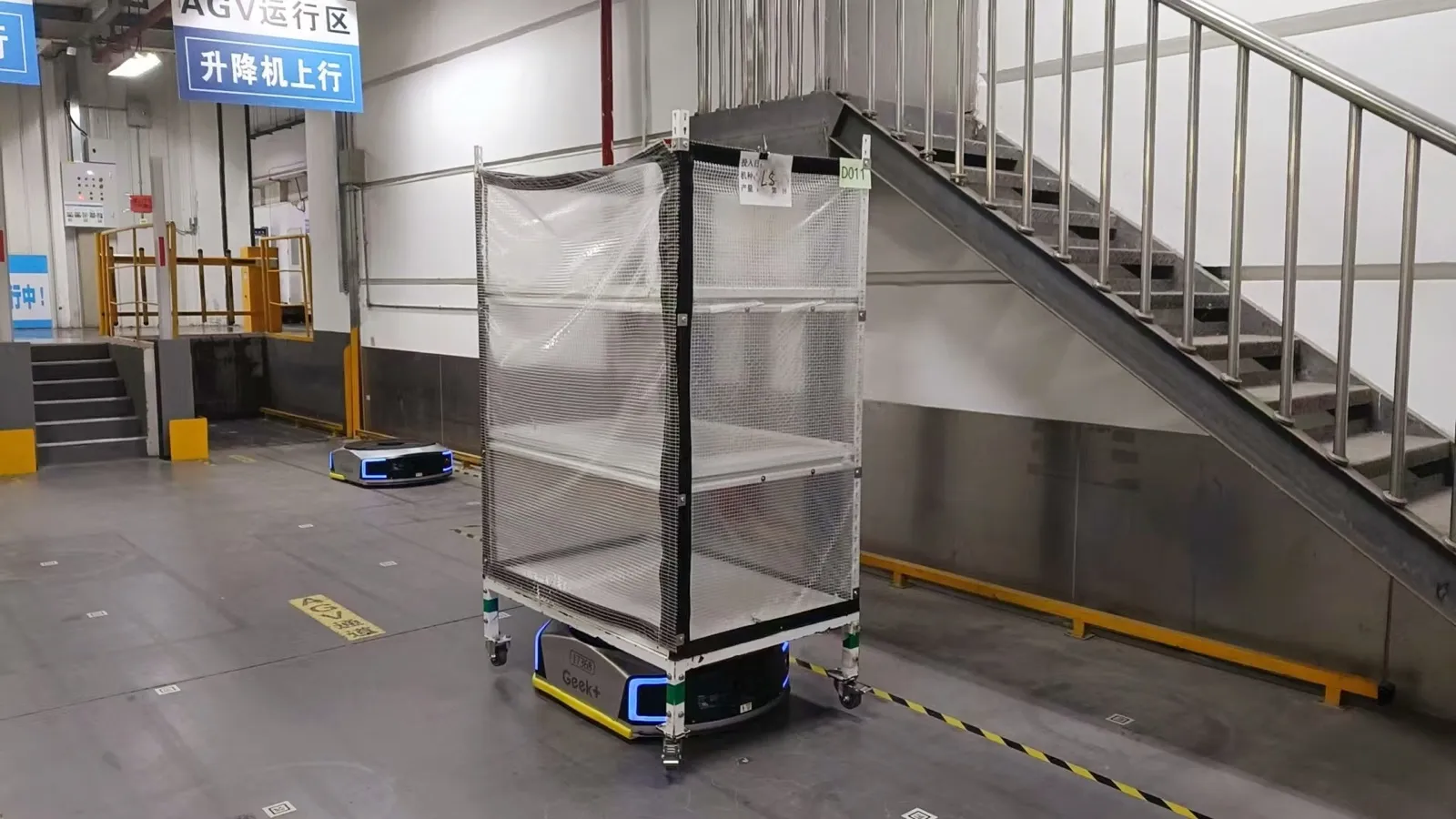
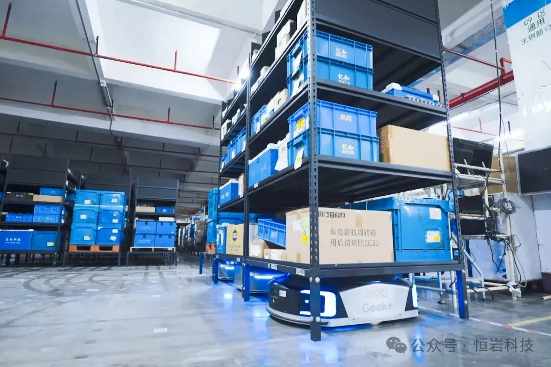
Autonomous Case-handling Robots coordinated through intelligent scheduling for goods-to-person picking
Precision automated storage for high-value 12-inch silicon wafers
Semiconductor · 99.9%+ Accuracy · 9 ACR Robots
Founded as Shanghai Shenhe Semiconductor in 2002, SICC (Zhongxin Jingyuan) has grown into one of China’s leading semiconductor silicon wafer manufacturers — alongside peers like Olympic Circuit in the electronics manufacturing space. The company supplies full-size wafers for logic chips, flash memory, DRAM, image sensors, and display driver ICs. As production scaled, their 1,200 m² wafer warehouse needed an upgrade to match the precision demands of 12-inch wafer handling.
The operating constraints SICC brought to the project.
High-value 12-inch wafers require extremely precise storage conditions and handling
Low inventory accuracy with manual processes risking costly errors
High physical demands on workers performing repetitive picking tasks
Disordered outbound sequencing caused time-consuming re-sorting downstream
Need for full traceability across every storage and retrieval operation
System components delivered for SICC, orchestrated by our WES.
Explore the HardwareAutonomous Case-handling Robots coordinated through intelligent scheduling for goods-to-person picking
Inter-group ordered + intra-group ordered outbound logic ensures pallets ship in the correct sequence, and bins within each pallet are also precisely ordered
Support batch outbound, single-bin picking, and cyclic replenishment modes
Outbound empty bins are immediately reused as inbound containers, reducing unnecessary robot trips
Real-time inventory updates, full task visibility, dynamic robot scheduling, and complete outbound traceability
In the semiconductor sector, CCMC demonstrates how full-chain automation extends from production lines to finished goods shipping.
Get a Similar AssessmentInventory accuracy reached 99.9%+ with real-time digital tracking
Storing semiconductor wafers is not warehousing. It is environmental engineering with a logistics layer on top.
A silicon carbide wafer is a disc thinner than a credit card, worth thousands of dollars, and sensitive to conditions that standard warehouses do not even measure. Temperature fluctuations cause thermal stress that creates micro-fractures invisible until the wafer fails during downstream processing. Humidity above threshold levels triggers surface oxidation that degrades electrical properties. Vibration during transport can chip wafer edges, turning a finished product into expensive scrap.
SICC produces silicon carbide wafers for power semiconductor applications — electric vehicles, renewable energy inverters, industrial motor drives. Each wafer passes through dozens of process steps over weeks of manufacturing. The storage system sits between those steps, holding work-in-progress inventory that represents significant accumulated processing cost.
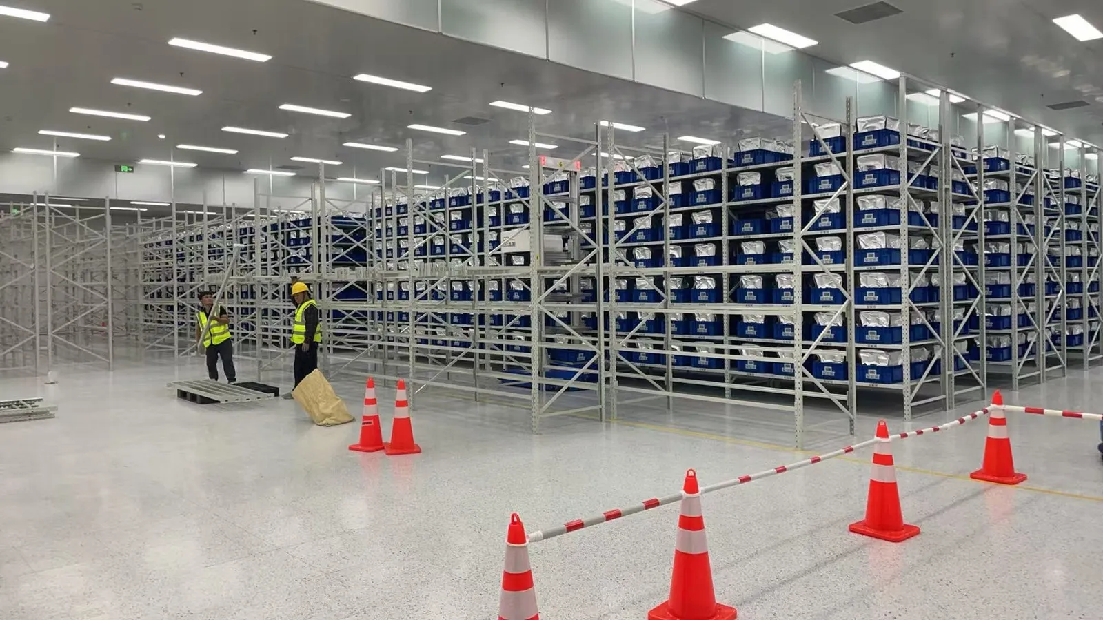
When we built SICC’s precision storage system, the environmental specifications drove every design decision before throughput or capacity entered the conversation. The hardware infrastructure operates inside a controlled environment where temperature, humidity, and particle counts are maintained at semiconductor fabrication standards — not warehouse standards.
Maintaining cleanroom conditions in a static room is well-understood engineering. Maintaining those conditions inside a dynamic storage system where robots move continuously, doors open and close, and totes cycle in and out is a different problem.
Every robot movement displaces air. Every door cycle exchanges atmosphere between zones. Every conveyor belt generates friction particles at a microscopic level. The WES coordinates with the environmental control system to manage these interactions — scheduling high-traffic operations during periods when the HVAC system has maximum recovery capacity, routing robots through paths that minimize door cycles, and monitoring particle counts at zone boundaries to detect contamination events before they propagate.
In our experience, the environmental integration layer consumed roughly 30% of the total engineering effort on this project. Standard warehouse automation projects spend zero time on this — the air is just air. In semiconductor storage, the air is a controlled process variable as critical as the robots themselves.
Each wafer carries a laser-marked ID that links to its complete processing history. The storage system extends that traceability chain by recording every environmental condition the wafer experienced during storage — temperature logs, humidity readings, time-in-storage, and the specific position coordinates where the wafer resided.
If a downstream process step reveals a defect pattern, engineers can query the storage history to determine whether affected wafers shared a storage zone during a period when environmental parameters drifted. This forensic capability has identified root causes that would be invisible without granular storage telemetry.
The WES maintains this data automatically as part of normal operations. No manual logging, no barcode scanning at checkpoints, no paper travelers attached to wafer carriers. The ASRS system overview covers the foundational tracking capabilities that semiconductor applications extend to this level of detail.
For precision manufacturers in adjacent industries, the CCMC case shows full-chain semiconductor logistics at a different scale. The Carl Zeiss case demonstrates comparable precision handling for optical components. Our solutions page outlines how we scope projects where environmental control is a primary requirement.
The WES enforces material segregation rules that prevent incompatible wafer types from sharing storage zones. Carrier types are matched to wafer specifications — a carrier designed for 6-inch wafers physically cannot accept 8-inch wafers, and the system rejects mismatched assignments at the software level before any physical movement occurs. Zone-level environmental profiles can be tuned independently, so different areas of the storage system maintain different conditions if required by the material mix.
The system runs on uninterruptible power with generator backup. If environmental controls degrade beyond threshold, the WES executes a controlled shutdown sequence — completing in-progress movements to safe positions, sealing zone boundaries to preserve conditions, and alerting facility management. Wafers in transit return to their last known-good storage position rather than stopping mid-path in an uncontrolled corridor. Recovery protocols verify environmental conditions zone by zone before resuming operations. The mini-load ASRS guide covers the storage architectures that support this level of operational resilience.
Bare wafers and partially processed wafers require the strictest controls. Packaged semiconductors in sealed containers tolerate standard warehouse conditions for storage, though they still benefit from vibration control and precise handling during transport. The cost-benefit calculation depends on your product’s sensitivity and value per unit. Contact us with your material specifications for a requirements assessment.
Intelligent raw material warehouse for precision camera lens manufacturing
End-to-end automation from production line to finished goods shipping
Precision line-side material management and automated delivery
Tell us about your warehouse challenges — our team will design a tailored automation plan for you.